The Reshoring Thesis Becomes Concrete and Steel
The numbers are staggering by any measure: $42 billion in active semiconductor fabrication plant construction across the United States, representing the largest industrial construction program in American history. This figure encompasses projects that have broken ground, are under construction, or have received final investment decisions with construction start dates confirmed through 2027. When you include announced projects that have not yet reached final investment decision, the total pipeline approaches $80 billion.
The scale of these projects defies comparison with any previous wave of industrial construction. A single leading-edge semiconductor fab costs $15 billion to $25 billion — more than the most expensive sports stadium, more than the largest hospital campus, and roughly equivalent to building a small city's worth of commercial infrastructure in a single project.
For the commercial construction industry, fab construction represents a once-in-a-generation opportunity. But the complexity, scale, and technical requirements of these projects create challenges that only a handful of contractors are equipped to manage. Let us examine the data and the implications.
The Active Project Pipeline
The $42 billion in active US fab construction is concentrated among a small number of companies building at a handful of sites:
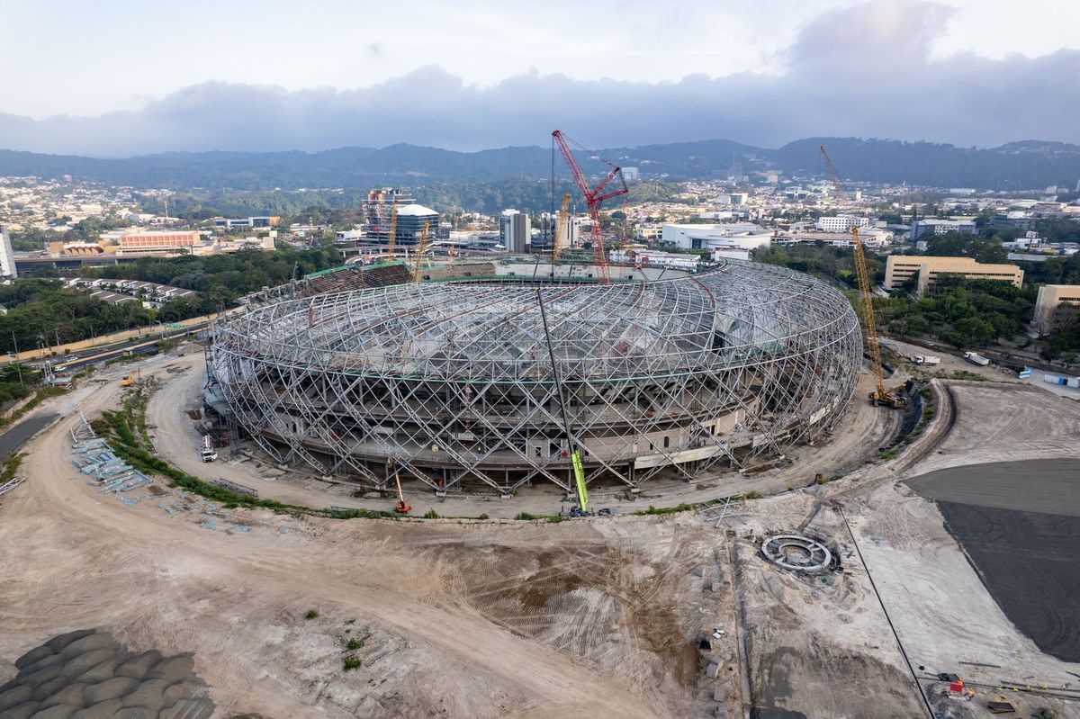
TSMC — Phoenix, Arizona: $65 billion total announced investment, approximately $20 billion in active construction. TSMC's Arizona complex will ultimately include multiple fabs producing chips at process nodes from 4nm to 2nm. The first fab (Fab 21, Phase 1) began production in early 2025, with Phase 2 under construction and Phase 3 in early site preparation. The combined complex represents the single largest private-sector construction project in US history.
Intel — Ohio, Arizona, Oregon, New Mexico: $30 billion total announced, approximately $12 billion in active construction. Intel's Ohio fab campus in Licking County is the company's most ambitious expansion, with two fabs under construction on a 1,000-acre site. Additional expansion is underway at Intel's existing campuses in Chandler, Arizona and Hillsboro, Oregon. Intel's projects are notable for their integration of advanced packaging facilities alongside traditional fabrication, reflecting the increasing importance of chip packaging in semiconductor performance.
Samsung — Taylor, Texas: $17 billion announced, approximately $6 billion in active construction. Samsung's Taylor fab, its first new US manufacturing site in decades, is under construction on a 1,200-acre site near Austin. The facility will produce advanced logic chips at 4nm and below, with production planned for late 2026.
Micron — Boise, Idaho and Clay, New York: $15 billion announced, approximately $3 billion in active construction. Micron's memory chip fabs represent the US strategy for maintaining domestic memory chip production capacity. The Clay, New York facility — supported by $6.1 billion in CHIPS Act funding — is in early construction, with the Boise expansion further advanced.
GlobalFoundries, Texas Instruments, and others account for the remaining $1 billion in active construction, primarily through expansion and modernization of existing facilities producing mature-node chips for automotive, industrial, and defense applications.
Construction Cost Anatomy
The cost structure of semiconductor fab construction is unlike any other building type. The numbers tell the story:
Cleanroom construction: 35% to 45% of total project cost. The cleanroom is the heart of a semiconductor fab — a controlled environment where temperature, humidity, vibration, and particulate contamination are maintained at levels vastly more stringent than any other built environment. A Class 1 cleanroom (fewer than 1 particle per cubic foot of air) costs $1,500 to $2,500 per square foot to construct. A single advanced-logic fab requires 300,000 to 500,000 square feet of cleanroom space, translating to $450 million to $1.25 billion in cleanroom construction costs alone.
The cleanroom construction scope includes ultra-flat raised floors (flatness tolerances of 0.5mm over 3 meters), vibration isolation systems (to protect equipment that operates at nanometer-scale precision), HEPA and ULPA filtration systems, precise temperature and humidity control (typically 68 degrees F plus/minus 0.5 degrees with 45% relative humidity plus/minus 2%), and the structural systems designed to support the extreme loads imposed by fab equipment.
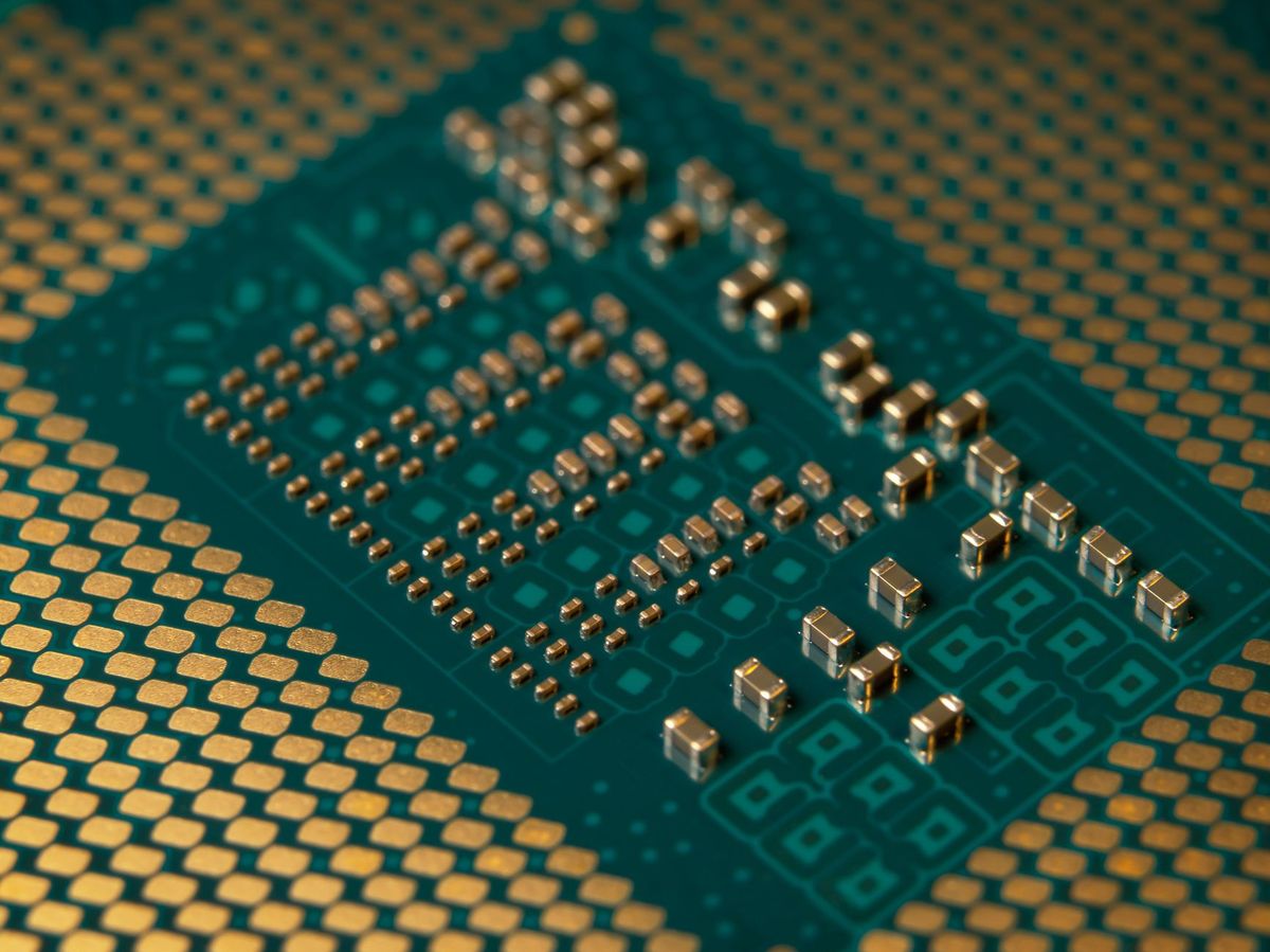
Process equipment installation: 25% to 35% of total project cost. The tools that actually make chips — lithography systems, etching equipment, deposition systems, metrology tools — cost $3 billion to $8 billion per fab. A single EUV lithography system from ASML costs $350 million and weighs 180 tons. Installing this equipment requires specialized rigging, ultra-clean assembly procedures, and extensive calibration. Equipment installation is typically performed by the equipment manufacturers' own teams, but the construction contractor provides the infrastructure — utilities, connections, structural support — that the equipment requires.
Building shell and site infrastructure: 15% to 20% of total project cost. The fab building itself is a massive reinforced concrete structure — typically 1 million to 3 million square feet of total floor area across multiple levels. The building must accommodate enormous electrical loads (a leading-edge fab consumes 100 to 200 megawatts of power — comparable to a small city), vast quantities of ultrapure water (2 million to 5 million gallons per day), and specialty gas systems that distribute dozens of process gases at precise pressures and purities.
Utility and infrastructure: 10% to 15% of total project cost. Fab sites require dedicated electrical substations, water treatment and recycling facilities, wastewater treatment systems, chemical storage and distribution systems, and backup power generation. The utility infrastructure for a major fab complex can cost $1 billion to $2 billion and may require upgrades to regional utility infrastructure that are funded jointly by the fab operator and the local utility.
The Workforce Challenge
The sheer scale of fab construction has created a labor demand that exceeds anything the construction industry has previously experienced in concentrated geographic areas. At peak construction, a single fab project employs 5,000 to 12,000 construction workers. When multiple projects are under construction simultaneously in the same region — as is the case in central Arizona with TSMC and Intel projects — the combined labor demand reaches 20,000 to 30,000 workers.
The workforce challenge manifests in several ways:
Skilled trade shortages. Fab construction requires electricians, pipefitters, iron workers, concrete finishers, and cleanroom specialists in quantities that exceed the local labor supply in every market where fabs are being built. Contractors are recruiting workers from across the country and, in some cases, internationally. Per diem payments, travel allowances, and retention bonuses have become standard, adding 15% to 25% to base labor costs.
Specialized skill requirements. Cleanroom construction, ultrapure water system installation, specialty gas piping, and vibration-sensitive concrete placement all require training and experience that most construction workers lack. The training pipeline for these specialties is limited, creating bottlenecks that have delayed project schedules on multiple active fab projects.
Competition with other mega-projects. Fab construction competes for workers with data center construction, battery plant construction, LNG facility construction, and other mega-projects that are simultaneously underway across the country. The total demand for skilled construction labor from industrial mega-projects exceeds 150,000 workers nationally — a significant fraction of the total industrial construction workforce.
CHIPS Act: The Government Catalyst
The CHIPS and Science Act of 2022 provides $52.7 billion in federal funding for semiconductor manufacturing, research, and workforce development. The manufacturing incentives — primarily direct subsidies and investment tax credits — have been the catalyst for the current wave of fab construction.
Through Q1 2026, the Commerce Department has awarded approximately $30 billion in CHIPS Act grants and loans to semiconductor manufacturers. The awards include both direct grants (typically covering 5% to 15% of total project cost) and loan guarantees that reduce the cost of financing. The 25% investment tax credit for semiconductor manufacturing equipment provides additional economic incentive.
The CHIPS Act has been effective in attracting investment. Industry analysts estimate that the $52.7 billion in federal funding has catalyzed approximately $250 billion in total announced private investment — a leverage ratio of roughly 5 to 1 that represents exceptional return on public investment.
However, the program is not without challenges. The application and review process has been slow, with some companies waiting 12 to 18 months for award decisions. Environmental review requirements under NEPA have added time and complexity. And the workforce development provisions — while well-intentioned — have not yet produced the volume of trained workers needed to support the construction and operation of the funded facilities.
Regional Economic Impact
The concentration of fab construction in specific regions is creating significant economic effects that extend well beyond the construction sites:
Housing demand. Each major fab project creates demand for 2,000 to 5,000 permanent jobs, plus the construction workforce during the building phase. This employment growth drives housing demand that has strained local markets. In the Phoenix metro area, the combined TSMC and Intel workforce has contributed to a 12% increase in housing demand in the east Valley, driving residential construction activity and home price appreciation.
Infrastructure investment. Fab projects require supporting infrastructure — roads, water systems, electrical grid upgrades, schools, healthcare facilities — that must be constructed concurrently. The infrastructure investment associated with a major fab complex typically equals 10% to 20% of the fab construction cost, creating additional construction opportunity but also placing demands on local governments and utilities.
Supply chain clustering. Semiconductor supply chain companies — specialty chemical manufacturers, gas suppliers, equipment service providers, and packaging companies — tend to locate near fab sites, creating additional construction demand. The clustering effect around the TSMC Arizona complex has already generated over $2 billion in additional supply chain construction investment.
Risk Factors
The fab construction boom carries risks that the industry should monitor:
Demand cyclicality. The semiconductor industry is inherently cyclical, and the current investment wave is based on projections of growing chip demand driven by AI, IoT, and EV applications. If demand growth falls short of projections, some of the announced capacity additions could be delayed or scaled back.
Geopolitical risk. The CHIPS Act was motivated by national security concerns about semiconductor supply chain concentration in Taiwan and South Korea. A resolution of US-China tensions could reduce the urgency of domestic reshoring, potentially affecting future fab investment decisions.
Construction cost escalation. The concentration of mega-projects has driven construction cost inflation in the regions where fabs are being built. In central Arizona, commercial construction costs have increased 18% to 22% over the past two years, significantly above national averages. Continued cost escalation could affect the economics of projects that have not yet reached final investment decision.
Despite these risks, the structural case for US semiconductor manufacturing investment remains strong. The bipartisan political support for the CHIPS Act, the national security imperative, and the growing demand for leading-edge chips all support continued investment in domestic fab capacity.
For the commercial construction industry, $42 billion in active projects — with a potential pipeline of $80 billion — represents the most significant industrial construction opportunity in a generation. The contractors who develop the specialized capabilities required for fab construction will be positioned for a decade or more of sustained demand. The numbers are clear: semiconductor fab construction is not a wave — it is a structural transformation of the American industrial landscape.
The Quality Standard: Why Fab Construction Is Different
What distinguishes semiconductor fab construction from other industrial building types is the uncompromising quality standard. In conventional construction, a tolerance of plus or minus one-eighth inch is considered precise. In semiconductor fab construction, tolerances are measured in millimeters — and in the cleanroom environment, in fractions of a millimeter.
The concrete floor slab in a fab cleanroom must achieve flatness specifications (FF values of 50 to 100) that exceed the standards for any other building type. Vibration isolation requires that the floor slab be decoupled from the building structure, with vibration levels measured in micro-inches per second — magnitudes that are imperceptible to human senses but potentially catastrophic for equipment operating at the nanometer scale.
The cleanroom air handling system must maintain air cleanliness levels that border on the impossible: Class 1 cleanrooms allow no more than one particle of 0.5 microns or larger per cubic foot of air. To achieve this, the air handling system recirculates the entire volume of the cleanroom 300 to 600 times per hour through ULPA filters with 99.999% efficiency. The system must operate continuously, and any interruption in filtration — even for minutes — can contaminate wafers that represent millions of dollars in product value.
The MEP piping systems in a fab carry ultrapure water (with purity levels measured in parts per trillion), specialty gases (delivered at precise pressures and flow rates through electropolished stainless steel piping), and chemical slurries used in the manufacturing process. Every pipe joint must be welded, inspected, and tested to standards that exceed pharmaceutical and nuclear facility requirements.
This quality standard creates a self-selecting group of contractors — the firms that can meet fab construction requirements have invested years in developing the workforce, the quality management systems, and the project management capabilities needed for this work. The barriers to entry are real and substantial, and they create market protection for the contractors who have cleared them.
The $42 billion pipeline represents not just construction volume but construction complexity at the highest level the industry can deliver. For the firms capable of this work, the opportunity is generational.
Frequently Asked Questions
What is driving semiconductor fab construction us growth in 2026?
According to the latest industry data, semiconductor fab construction us is showing notable trends in 2026. Current figures indicate $42 billion, which represents a significant benchmark for contractors and developers planning projects this year. Regional variations apply, so checking local market conditions remains essential for accurate budgeting.
How much does semiconductor fab construction us cost per square foot?
Regional analysis of semiconductor fab construction us reveals uneven distribution across U.S. markets. The data point of $80 billion highlights the scale of activity, with Sun Belt and high-growth metro areas generally leading in volume. Contractors expanding into new territories should evaluate local demand indicators before committing resources.
Which markets are seeing the most semiconductor fab construction us?
The trajectory for semiconductor fab construction us tells an important story when viewed against historical benchmarks. With the latest data showing $15 billion, the trend has clear implications for project feasibility, bidding accuracy, and resource allocation across the construction sector.