Semiconductor fabrication facility construction in the United States has entered an era without modern precedent. The CHIPS and Science Act, signed into law in August 2022, authorized $52.7 billion in federal incentives for domestic semiconductor manufacturing, and that money is now flowing into construction sites across the country. As of Q1 2026, the Commerce Department's CHIPS Program Office has awarded over $36 billion in direct grants and $12 billion in federal loans to semiconductor companies, triggering combined private-sector capital commitments exceeding $450 billion through 2030. The numbers tell a different story than the technology headlines — this is fundamentally a construction story, and the construction industry is the bottleneck between policy ambition and fabricated silicon.
According to the Semiconductor Industry Association (SIA) and FMI Capital Advisors, total semiconductor facility construction spending in the United States will reach approximately $52 billion in 2026 — making it the single largest manufacturing construction subsector in the country. This figure encompasses new fab construction, cleanroom buildout, process tool installation, and supporting infrastructure including power generation, water treatment, and chemical delivery systems. For construction firms with industrial or high-tech facility experience, the semiconductor construction boom represents the largest single-sector opportunity in a generation.
The Major Projects: Who's Building Where
The semiconductor construction landscape is dominated by a handful of mega-projects from the world's leading chipmakers, each representing billions of dollars in construction investment.
Taiwan Semiconductor Manufacturing Company (TSMC) — Phoenix, Arizona. TSMC's Arizona complex represents the largest single foreign direct investment in American manufacturing history. The project encompasses three fabrication facilities on a 1,100-acre campus in north Phoenix. Fab 1 (N4 process technology) began production in early 2025 after overcoming construction delays. Fab 2 (N3E and N2 process technology) is under active construction with completion targeted for 2028. Fab 3 (A16 process, the most advanced node) is in early construction phases. Total investment exceeds $65 billion, with CHIPS Act grants of $6.6 billion and federal loans of $5 billion. At peak construction, the site employs approximately 12,000 construction workers — one of the largest active construction workforces on any single project site in the country.
Intel Corporation — Arizona, Ohio, New Mexico, Oregon. Intel is executing a multi-state construction program funded by $8.5 billion in CHIPS grants and $11 billion in federal loans — the largest single CHIPS award. In Chandler, Arizona, Intel is constructing two new fabs (Fabs 52 and 62) at its Ocotillo campus, with combined investment exceeding $20 billion. In New Albany, Ohio, Intel is building a greenfield manufacturing campus with initial investment of $28 billion for two fabs, with site infrastructure construction underway and fab shell construction advancing. In Rio Rancho, New Mexico, Intel is modernizing its existing Fab 9 for advanced packaging operations at a cost of approximately $3.5 billion. In Hillsboro, Oregon, Intel continues facility upgrades at its D1X fab and Gordon Moore Park campus.
Samsung Electronics — Taylor, Texas. Samsung is constructing a new advanced logic fab in Taylor, Texas with an investment of approximately $17 billion, supplemented by a $6.4 billion CHIPS grant. The fab is designed for Samsung's Gate-All-Around (GAA) transistor technology at 2nm and below. Construction is well advanced, with cleanroom buildout in progress and tool installation beginning. Samsung has also announced plans for a second fab at the Taylor site, with potential investment exceeding $25 billion for the full campus.
Micron Technology — Clay, New York and Boise, Idaho. Micron is constructing a massive DRAM memory fabrication complex in Clay, New York (near Syracuse), with total planned investment of up to $100 billion over 20 years — the largest private investment commitment in New York State history. Initial phase construction (two fabs) carries an investment of approximately $20 billion, supported by $6.1 billion in CHIPS grants and $7.5 billion in federal loans. Site preparation and infrastructure construction is underway. In Boise, Idaho, Micron is investing approximately $15 billion in fab modernization and expansion.
Texas Instruments — Sherman, Texas and Lehi, Utah. TI is building four new 300mm analog semiconductor fabs, with $1.6 billion in CHIPS grants. The Sherman, Texas campus (SM1 and SM2 fabs) represents approximately $18 billion in total investment. The Lehi, Utah fab (LFAB2) adds another $3 billion. TI's fabs, while less technologically complex than leading-edge logic fabs, are massive construction projects involving millions of square feet of cleanroom and manufacturing space.
GlobalFoundries — Malta, New York and Burlington, Vermont. GF received $1.5 billion in CHIPS grants to expand its Malta fab (Fab 8) and modernize its Burlington facility. Fab 8 expansion adds approximately 150,000 square feet of cleanroom and increases wafer production capacity by 35%.
Anatomy of Fab Construction
A modern semiconductor fab is among the most complex and expensive buildings ever constructed. Understanding the construction scope is essential for contractors evaluating the market.
The building shell — typically a massive reinforced concrete and steel structure — provides the structural and environmental envelope for the cleanroom and support systems. A leading-edge logic fab building shell is typically 1.5 to 2.5 million square feet across multiple levels, with floor-to-floor heights of 20 to 30 feet to accommodate the subfab (the level below the cleanroom where process utilities are distributed) and the interstitial space above the cleanroom (where air handling and filtration systems are located). Shell construction for a single fab building costs approximately $1.5 to $3 billion and takes 18 to 24 months.
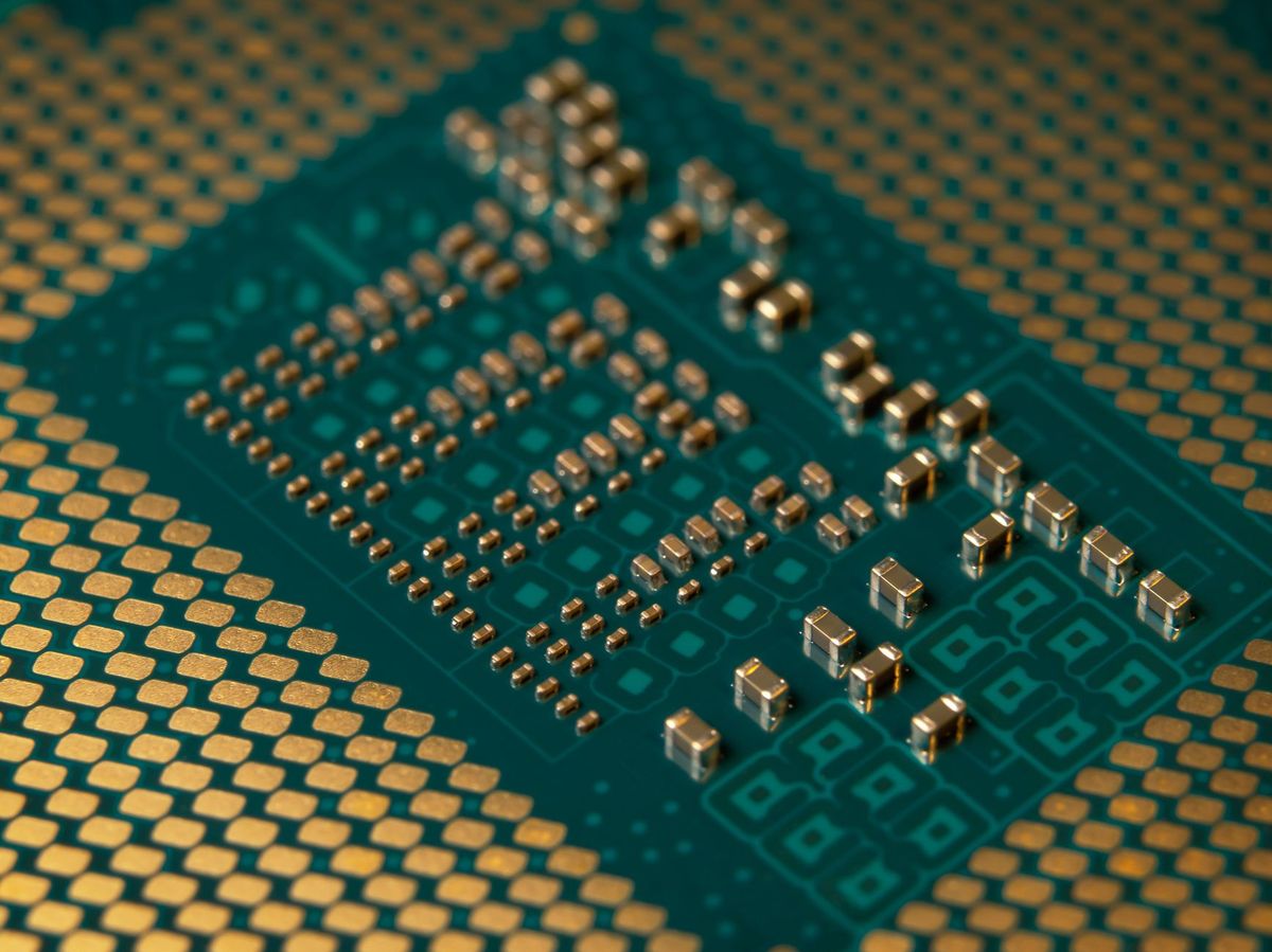
Cleanroom construction involves the installation of the controlled environment where semiconductor wafers are processed. Modern fabs require ISO Class 1 to ISO Class 5 cleanrooms (the most stringent classification allows fewer than 10 particles per cubic meter at 0.1 micrometer size — orders of magnitude cleaner than a hospital operating room). Cleanroom construction includes raised access floor systems with pedestals and panels, cleanroom wall and ceiling systems with sealed panel construction, high-efficiency particulate air (HEPA) and ultra-low particulate air (ULPA) filtration systems in fan filter units (FFUs) covering the entire cleanroom ceiling, static-dissipative flooring to prevent electrostatic discharge damage to sensitive chips, and precisely controlled temperature (typically 68 degrees F plus or minus 0.5 degrees) and humidity (45% RH plus or minus 2%) systems. Cleanroom construction costs approximately $2,000 to $5,000 per square foot of cleanroom area — among the highest per-square-foot construction costs of any building type.
Process utility systems — the "plumbing" of a semiconductor fab — are extraordinarily complex and account for approximately 30 to 35% of total construction cost. These systems include ultra-pure water (UPW) production and distribution (18.2 megohm-cm resistivity water at flow rates of 500 to 2,000 gallons per minute), specialty gas delivery systems for dozens of process gases including toxic, corrosive, and pyrophoric gases, chemical delivery systems (bulk and point-of-use) for hundreds of process chemicals, exhaust and abatement systems for managing hazardous process byproducts, process cooling water and chilled water systems, and compressed dry air and nitrogen systems. Process utility installation requires specialized piping contractors experienced with high-purity welding (orbital TIG welding for stainless steel and specialty alloy piping), double-containment piping systems, and rigorous cleanliness protocols.
Electrical infrastructure for a modern fab is staggering in scale. A single leading-edge logic fab consumes 60 to 100 megawatts of electrical power — equivalent to a small city. The electrical construction scope includes utility substation construction (often multiple substations at 138 kV or 230 kV), medium-voltage distribution at 4.16 kV to 15 kV, step-down transformation and low-voltage distribution, uninterruptible power supply (UPS) systems protecting critical process loads, emergency generator plants (typically 20 to 40 MW of diesel or natural gas generator capacity), and power monitoring and management systems. Electrical construction costs for a single fab can exceed $500 million.
Workforce: The Critical Constraint
The semiconductor construction workforce challenge is acute. The construction labor pool for fab construction is specialized — the cleanroom, process utility, and electrical work requires trades with specific experience that limits the available workforce.
According to CHIPS for America's workforce analysis, the semiconductor construction boom will require an additional 40,000 to 50,000 construction workers at peak activity (projected for 2026-2028), with the highest demand for pipe fitters and welders (especially those qualified for orbital TIG welding on high-purity piping systems), electricians with medium-voltage and industrial controls experience, ironworkers for structural steel and equipment rigging, HVAC and refrigeration technicians for cleanroom environmental systems, and sheet metal workers for ductwork and cleanroom panel installation.
The geographic concentration of fab construction — primarily in Arizona, Ohio, Texas, and New York — is creating intense local labor market competition. Construction wages in the Phoenix metropolitan area have increased 18 to 22% since 2022, driven largely by the TSMC and Intel projects competing for the same workforce. Similar dynamics are emerging in central Ohio around the Intel site and in central Texas around the Samsung and TI projects.
Contractors are responding with aggressive recruitment, wage escalation, and worker housing and transportation programs. Several fab projects have established dedicated worker housing developments near construction sites to attract out-of-state construction workers — a practice historically associated only with the largest remote infrastructure projects.
What This Means for Your Crew
Semiconductor fab construction is the highest-value construction market in the country on a per-square-foot basis, and the demand will persist through at least 2030. But the barriers to entry are real — fab construction requires specific capabilities that distinguish it from standard industrial or commercial construction.
If you're a mechanical contractor or pipe fitting firm, the high-purity piping scope at semiconductor fabs is the most lucrative construction specialty available. Orbital TIG welding certification, experience with double-containment piping systems, and cleanroom construction protocols are the key qualifications. The investment in training and certification is substantial but the returns are compelling — high-purity piping contractors on fab projects command hourly rates 30 to 50% above standard industrial piping work.
If you're an electrical contractor, fab electrical construction requires medium-voltage and power distribution experience beyond what most commercial electricians possess. Firms with industrial power experience — particularly those who have worked on data centers, industrial plants, or utility substations — have transferable capabilities. The data center construction boom at $32 billion has created a large pool of electricians with the power distribution skills relevant to fab work.
If you're a general contractor, fab construction general contracting is dominated by a small number of specialized firms — Hensel Phelps, M+W Group (now Exyte), Jacobs, and Fluor are the primary general contractors on leading-edge fab projects. Subcontracting to these primes is the most practical entry point for firms seeking fab construction experience.
Frequently Asked Questions
How much does it cost to build a semiconductor fab?
A modern leading-edge logic fab (producing chips at 5nm, 3nm, or 2nm process nodes) costs approximately $15 to $28 billion total, including building shell construction ($1.5 to $3B), cleanroom and facility systems ($3 to $6B), process tool procurement and installation ($8 to $15B), and site infrastructure ($1 to $3B). Memory fabs (DRAM and NAND flash) cost approximately $8 to $15 billion. Analog and specialty fabs cost $3 to $8 billion. These figures include both construction costs and process equipment costs — the construction portion (excluding process tools) typically represents 40 to 55% of total investment.
How long does it take to build a semiconductor fab?
The construction timeline for a leading-edge fab from groundbreaking to production qualification typically spans 3 to 4 years. Site preparation and foundation construction takes approximately 6 to 12 months. Building shell construction takes 12 to 18 months. Cleanroom and facility systems buildout takes 12 to 18 months (overlapping with shell construction). Process tool installation and qualification takes 12 to 18 months (overlapping with facility buildout). TSMC's experience in Taiwan demonstrates that fab construction can be compressed to approximately 24 months from start to production, but the company's initial U.S. experience showed that achieving this timeline in the American construction environment required adaptation.
What is the CHIPS Act and how much construction funding does it provide?
The CHIPS and Science Act provides $52.7 billion in federal incentives for domestic semiconductor manufacturing. Of this total, approximately $39 billion is dedicated to manufacturing incentives (direct grants and loans to semiconductor companies for fab construction and expansion), $11 billion for R&D programs, and $2.7 billion for workforce development and international cooperation. As of Q1 2026, the Commerce Department has awarded over $36 billion in grants and $12 billion in loans, triggering more than $450 billion in total private sector investment commitments. The construction portion of these commitments — approximately 40 to 55% of total investment — translates to an estimated $180 to $250 billion in semiconductor construction spending through 2030.
Where are semiconductor fabs being built in the US?
The geographic concentration of fab construction reflects a combination of state incentive packages, labor market access, utility infrastructure, and existing semiconductor industry presence. Arizona (TSMC, Intel) is the largest market with over $85 billion in combined investment. Texas (Samsung, Texas Instruments) has approximately $55 billion in investment. Ohio (Intel) has $28 billion in initial investment with plans for up to $100 billion. New York (Micron, GlobalFoundries) has over $100 billion in planned long-term investment. Other states with significant fab construction activity include Idaho (Micron), Oregon (Intel), New Mexico (Intel), Utah (Texas Instruments), and Vermont (GlobalFoundries).
What to Watch
The semiconductor construction boom will shape American industrial construction for the rest of this decade. Watch for CHIPS Act Phase 2 discussions — with the initial $39 billion in manufacturing incentives largely committed, industry and policymakers are already discussing additional federal investment to sustain the reshoring momentum. Watch construction cost trends — fab construction costs have increased approximately 15 to 20% since 2022 due to labor competition and material cost escalation, and further increases could challenge project economics. Watch workforce development programs — the CHIPS workforce initiative is funding community college and apprenticeship programs in fab construction states, and the graduates of these programs will determine whether the construction industry can execute at the required scale. And monitor the broader construction spending forecast of $2.1 trillion — semiconductor fab construction is the most capital-intensive subsector within this total, and its success or failure will materially affect the overall construction economy.